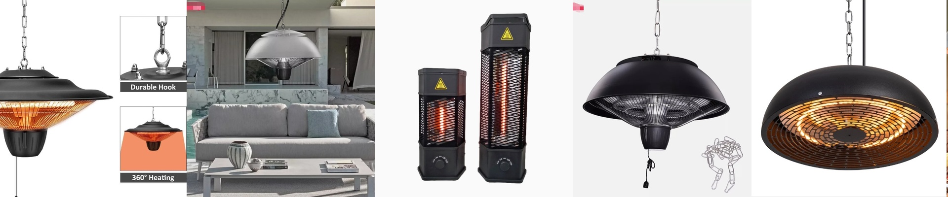

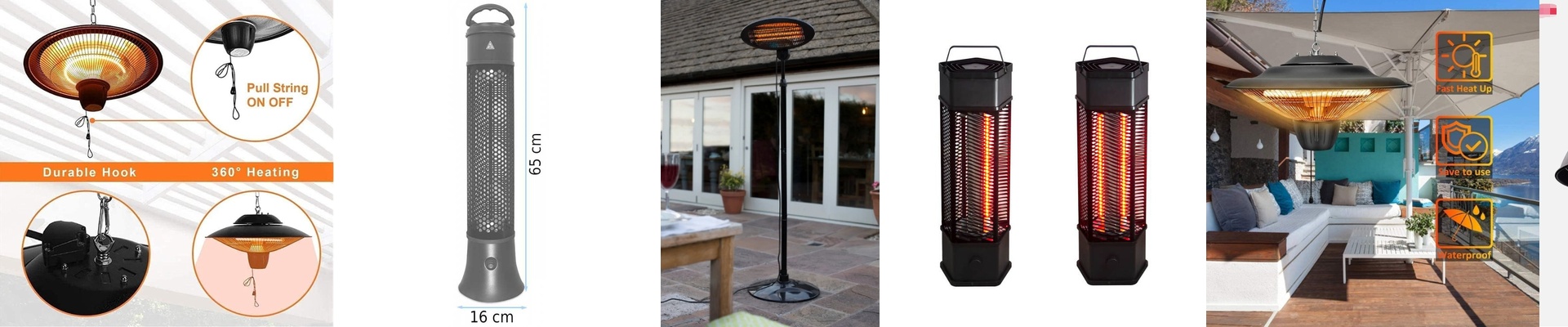
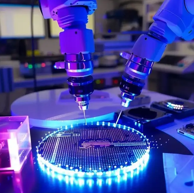
On the lithography floor, you know how it goes. A soft bake or hard bake profile that drifts even half a degree can pull critical dimensions by nanometers. You see it right away—scumming, footing, bridging—then you’re staring at scrap wafers. We built our Photoresist curing infrared lamps to keep thermal behavior honest, shift after shift, even through PM windows. What matters, technically We run short-wave infrared emitters with a fast-response quartz envelope. The heat goes straight into the photoresist layer without baking the carrier, so you get wafer-level uniformity of ±0.1°C and bake curves that lock in your process window. The system stays clean—zero particle generation, good for cleanroom Class 1–100—and it plugs into standard SEMI interfaces. Output holds steady over 5,000+ hours, with less than 5% intensity drop. Photoresist processing is all about managing the thermal budget. The bake has to hit target quickly, sit steady, then release clean. Our lamps cut soak time and settle temperature within seconds, so you get more throughput without chasing higher energy draw. The same thermal profile repeats batch after batch, lot after lot. That predictability is what keeps CD control tight and yield where it should be. On 7×24 lines, the design keeps unplanned downtime at zero, and maintenance stays on schedule instead of turning into panic fixes. A few things to keep in mind. Installation is straightforward, but alignment to the wafer plane and emitter-to-substrate distance have to be locked down within tight tolerances. If they aren’t, uniformity starts to drift. The lamp face runs hot, so thermal isolation and interlocks are mandatory. And you have to match the emitter spectrum to the photoresist absorption band—different resists need different NIR profiles, so we size the system accordingly.